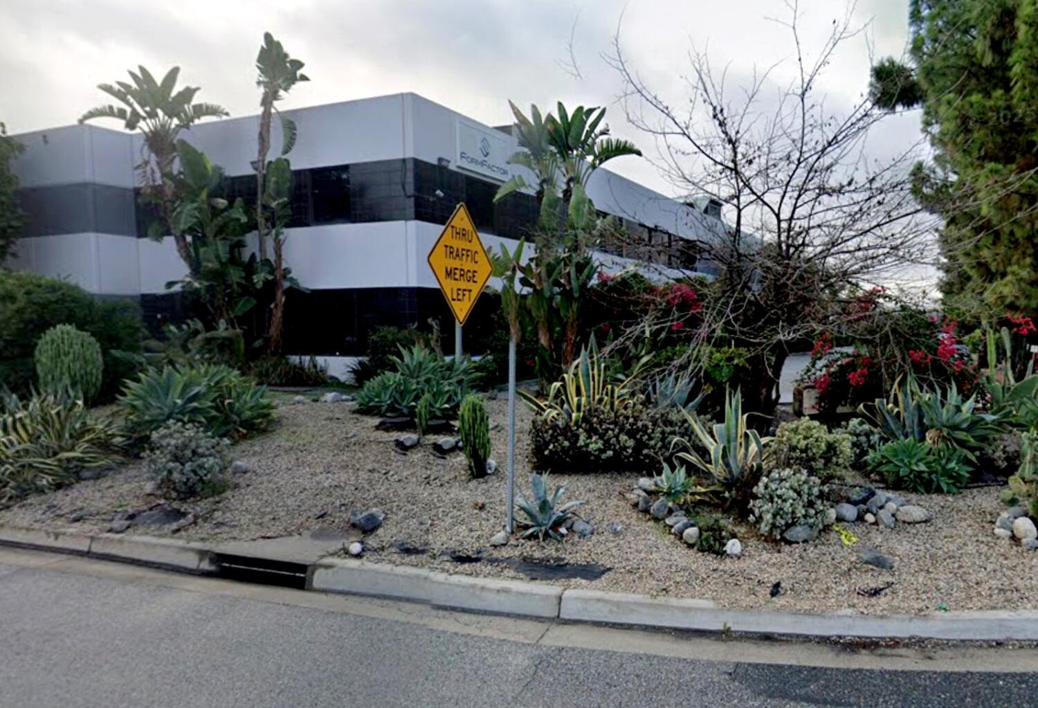
The announced reduction of 213 employees at FormFactor’s Livermore headquarters is not an isolated headcount adjustment but a lagging indicator of a fundamental shift in the semiconductor testing capital expenditure (CapEx) cycle. While surface-level reporting focuses on the immediate human impact, a rigorous analysis reveals a deeper misalignment between legacy electromechanical testing architectures and the rapid transition toward High-Bandwidth Memory (HBM3) and heterogeneous integration. This contraction serves as a case study in the "Inventory Correction Paradox," where record-high demand for AI-specific silicon fails to insulate upstream component suppliers from the cyclical volatility of the broader consumer electronics and PC markets.
The Mechanics of Testing Latency
To understand why a leading supplier of probe cards and wafer test equipment is trimming its workforce during a global AI boom, one must first deconstruct the Testing Value Chain (TVC). FormFactor operates at the intersection of wafer-level testing and final assembly. Their primary product—the probe card—is a bespoke, high-precision interface that connects the automated test equipment (ATE) to the individual die on a silicon wafer.
The economic viability of these operations depends on three distinct variables:
- Product Proliferation Rate: The frequency with which chip designers (NVIDIA, AMD, Intel) release new tape-outs. Each new chip architecture requires a custom probe card.
- Utilization-to-Obsolescence Ratio: The lifespan of a testing rig versus the volume of chips it processes.
- The Silicon Surface Area Constant: As chips move toward "chiplet" designs, the complexity of testing increases, but the number of physical contact points can consolidate, reducing the total unit volume of probe cards required for a given batch of transistors.
The current layoffs suggest a temporary decoupling where the surge in AI GPU production cannot compensate for the persistent glut in the mobile and client computing segments. When smartphone volumes stagnate, the demand for the specific probe cards used in those high-volume, low-margin applications collapses, creating an immediate revenue hole that low-volume, high-complexity AI components cannot yet fill.
The Three Pillars of Testing Volatility
The volatility impacting Bay Area semiconductor service providers stems from a structural "bullwhip effect" that begins at the retail level and amplifies as it moves toward the fabrication plant (fab).
I. The Heterogeneous Integration Bottleneck
Modern semiconductors are increasingly moving away from monolithic designs toward "Advanced Packaging." This involves stacking memory (HBM) directly onto logic units. While this improves performance, it shifts the "test burden" further down the line. If a company's headcount is heavily weighted toward traditional "sort and test" for monolithic dies, they face a structural surplus of labor as the industry moves toward Advanced Probe Stations and thermal management solutions.
II. The Cost Function of Precision Engineering
In the Livermore corridor, the cost of specialized labor is a fixed overhead that does not scale elastically with revenue. FormFactor’s decision to cut 13% of its local workforce suggests that the Marginal Cost of Talent has exceeded the Expected Yield per Employee in their current product mix. In a high-interest-rate environment, firms are forced to prioritize "Free Cash Flow per Head," a metric that punishes companies maintaining a bench of engineers for projects that are currently stalled in the design phase.
III. Geographical Arbitrage and Fab Proximity
There is an undeniable geographical tension. As Intel, TSMC, and Samsung build out "Silicon Heartland" fabs in Arizona, Ohio, and Texas, the necessity of maintaining massive engineering footprints in the high-cost San Francisco Bay Area diminishes. The "Proximity Premium"—the value added by being near the design centers in Silicon Valley—is being outweighed by the "Operational Tax" of California’s regulatory and cost environment.
Quantifying the Inventory Correction
The semiconductor industry is currently navigating a "Double-Bottom" recovery. While the 2023 downturn was driven by post-pandemic oversupply, the 2024-2025 period is defined by a transition in Wafer Starts Per Month (WSPM).
Total testing demand is a function of:
$$D_{test} = \sum (WSPM_{n} \times C_{n})$$
Where $n$ represents the node (e.g., 3nm, 5nm) and $C$ represents the complexity coefficient.
Even as $C$ increases due to AI requirements, a significant drop in $WSPM$ for legacy nodes (14nm to 28nm) used in automotive and industrial IoT has created a net deficit. FormFactor’s layoffs reflect a strategic pivot away from these "legacy" nodes. The company is likely reallocating its capital toward the "Front-End-of-Line" (FEOL) testing for 2nm and 3nm processes, which require fewer, but more expensive, human touchpoints and more automated, AI-driven optical inspection.
The Logic of Workforce Contraction
This reduction in force (RIF) follows a predictable pattern of Operational De-risking. When a technology firm identifies a permanent shift in the demand curve, it must execute a three-step compression:
- Elimination of Redundant R&D Pathways: Stopping work on "nice-to-have" testing architectures for markets with low CAGR (Compound Annual Growth Rate).
- Consolidation of Manufacturing Centers: Moving high-volume assembly to lower-cost regions (such as their facilities in Singapore or Germany) while retaining only "pathfinding" engineering in Livermore.
- Variable Cost Conversion: Transitioning from a heavy full-time equivalent (FTE) model to a more flexible, project-based engineering approach.
The 213 workers being released are likely the casualty of the second point. As the industry matures, the "art" of probe card manufacturing is being codified into "science"—meaning it can be automated or moved to regions where the cost of specialized labor is 40% lower.
Identifying the True Bottleneck
The real story isn't that FormFactor is shrinking; it's that the Testing Intensity Per Transistor is changing. In the previous era, you tested for "Is it broken?" In the AI era, you test for "How much heat can it handle before it fails?"
This shift from functional testing to thermal/parametric characterization requires a different kind of infrastructure. The existing workforce in Livermore was likely optimized for the former. Retraining a workforce of hundreds to handle the complexities of cryogenic testing (for quantum) or extreme-high-temperature testing (for power electronics) is often more expensive than a strategic "Reduction and Re-hire" cycle.
Strategic Play for the Semiconductor Services Sector
To survive the current transition, firms in the semiconductor testing space must move beyond the "Hardware-as-a-Product" model and adopt a "Throughput-as-a-Service" philosophy.
The first strategic imperative is the aggressive adoption of Digital Twin Testing. By creating a virtual model of the probe card and the wafer, engineers can simulate electrical interference before the first physical contact is made. This reduces the need for the large-scale physical prototyping teams that currently dominate Bay Area payrolls.
The second imperative is Diversification into the Power Semiconductor Vertical. As Silicon Carbide (SiC) and Gallium Nitride (GaN) become the standard for Electric Vehicles, the testing requirements differ wildly from traditional CMOS silicon. Companies that fail to pivot their workforce toward these high-voltage testing environments will find themselves over-staffed for a smartphone market that has reached peak saturation.
The third and most critical move is the Integration of Machine Learning into Automated Test Equipment (ATE). Instead of manual debugging of "false fails" on the test floor—a labor-intensive process—companies must implement edge-AI at the probe station to categorize defects in real-time. This structural shift inherently reduces the headcount required to maintain a high-yield production line.
The Livermore layoffs are the first major signal that the "Golden Era" of general-purpose semiconductor testing is ending. The industry is bifurcating into two segments: high-volume, low-margin automated commodity testing located near Asian assembly hubs, and hyper-specialized, low-volume "Extreme Physics" testing located near US research centers. FormFactor’s current contraction is a painful but necessary recalibration to fit into the latter.
Firms remaining in high-cost corridors must immediately audit their labor-to-revenue ratios and shed any divisions tied to the 10nm+ nodes, as those markets no longer support the overhead of a California-based engineering team. The focus must shift entirely to the Advanced Packaging Interface, where the highest margins and the most significant technical moats reside. Expect further "right-sizing" across the Bay Area as the industry realizes that AI demand, while massive, is more "labor-efficient" than the consumer electronics booms of the past decade.